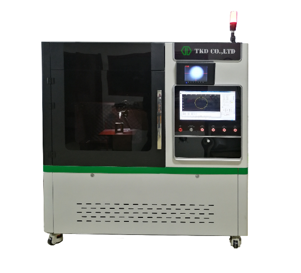
Silicon carbide (SiC) single crystal material, as a representative of the third-generation semiconductor material, has superior properties such as large band gap, high breakdown electric field, high thermal conductivity, high voltage, and can also meet the needs of radio frequency devices for high thermal conductivity and radiation resistance. They have great application prospects in the fields of electric vehicles, new energy, and communications. Silicon carbide is used as a substrate material. Due to its high hardness and difficulty in processing, the traditional cutter wheel cutting technology faces problems such as low processing efficiency, heavy environmental burden, and large material loss, resulting in high production costs and expensive prices. Scale application.
Silicon carbide materials are difficult to process;
High hardness, Mohs hardness distribution is 9.2 ~ 9.6;
High chemical stability, almost no reaction with any strong acid or alkali;

Silicon carbide is a group IV-IV binary compound semiconductor with strong ionic covalent bonds, stable bond energy, and excellent mechanical and chemical properties. The bandgap of the material, that is, the energy of the forbidden band, determines many properties of the device, including spectral response, radiation resistance, operating temperature, breakdown voltage, etc., and the bandgap width of silicon carbide is relatively large.
Since the most commonly used 4H-SiC has a band gap energy of 3.23 eV, it has good ultraviolet spectral response characteristics and is used to make ultraviolet light diodes. The critical breakdown electric field of SiC is much larger than that of ordinary semiconductor silicon and gallium arsenide, and its fabricated devices have excellent high withstand voltage characteristics.
The breakdown electric field and thermal conductivity determine the maximum power transmission capability of the device. The thermal conductivity of SiC is as high as 5w/(cmk), which is higher than that of many metals and is very suitable for high temperature, high power devices and circuits. Silicon carbide has good thermal stability and works at 300~600°C. Silicon carbide has high hardness and good wear resistance, and is often used for grinding and cutting other materials, which means that it is very difficult to cut and scribe silicon carbide substrates.
At present, there are mainly two types of silicon carbide wafers used in the production of electronic devices. The n-type conductive wafers have a thickness of 150-350 m and a resistivity of 0.010-0.028 cm 2 . The insulating wafer is 50-100 m thick and has a resistivity of 110 8 cm 2 , which is mainly used in microwave radio frequency, gallium nitride transistor and other fields. The characteristics and applications of several processing methods are studied for SiC wafer dicing used in the semiconductor industry.
Silicon carbide wafer cutting method
1. Grinding wheel scribing
The grinding wheel cutting machine rotates the blade at high speed through the aerostatic electric spindle to achieve strong grinding of materials. The blades used are coated with corundum particles. The Mohs hardness of corundum is 10, which is only slightly higher than that of SiC with a hardness of 9.5. Repeated low-speed grinding is not only time-consuming and laborious, but also causes frequent wear of the tool. For example, it takes 6 to 8 hours to cut a SiC wafer of 100 mm (4 inches) one by one, which is likely to cause chipping. Therefore, this traditional inefficient processing method is gradually replaced by laser cutting.
2. Full laser marking
Laser scribing refers to the process of irradiating the surface of a workpiece with a high-energy laser beam to locally melt and gasify the irradiated area, remove material, and realize cutting. Laser scribing non-contact processing, no mechanical stress damage, flexible processing methods, no tool loss and water pollution, low equipment maintenance costs. In order to prevent damage to the supporting film when the laser penetrates the wafer, a high-temperature ablated UV film is used.
At present, laser scribing equipment adopts industrial lasers, with three main wavelengths of 1 064 nm, 532 nm, and 355 nm, and pulse widths of nanoseconds, picoseconds, and femtoseconds. In theory, the shorter the laser wavelength and the shorter the pulse width, the smaller the thermal effect of processing, which is conducive to fine and precise processing, but the cost is relatively high. The 355 nm ultraviolet nanosecond laser is widely used due to its mature technology, low cost and small processing thermal effect. In recent years, 1 064 nm picosecond laser technology has developed rapidly and has been applied in many new fields with good results. Figure 1 and Figure 2 respectively compare the cutting effects of two lasers on SiC wafers.
The thermal effect of 355 nm ultraviolet laser processing is small, but the incompletely gasified slag adheres and accumulates in the cutting line, the cutting section is not smooth, and the attached slag is easy to fall off in the subsequent process, which affects the device performance. 1) The 1 064 nm picosecond laser adopts high power, high cutting efficiency, sufficient material removal, and uniform cross-section, but the thermal effect of processing is too large, and the chip design needs to ensure a wider cutting track.


 Whatsapp/wechat